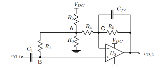
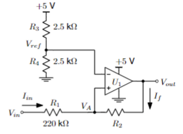
A still of the final device
Over the course of our labs of my Microelectronics II course, everyone was tasked to construct a device that measures pulse rate using a method called photoplethysmography (PPG) in groups of two. Up until now, most of my labs were largely independent of one each other in their content. This lab felt different: it was more of a semester-long project.
The final device schematic in LTspice
GIF of the final device functioning
Stage 1: Getting the Signal
The first stage of the device is to actually get the signal. To accomplish this, a combination of an infrared emitter and photodiode are placed in close proximity which then connect to a transimpedance amplifier. The datasheet for the infrared emitter was used to find the optimal value for RD1. Additional calculations were performed to find the best values for Cf and Rf. The current from the input of the amplifier is changed and amplified to a voltage output, where it can be fed into the proceeding stages. For the final product, the infrared emitter and photodiode were soldered on to a separate board. From there, the user places their finger on top of the two devices to detect their pulse.
The schematic of the first stage of the device
Stage 2: High-pass Filter and Amplification
The second stage of the device, in conjunction with the first stage, filters the signal incoming signal to allow frequencies around 1Hz through, attenuating frequencies below 0.1Hz and above 10Hz. The filtered signal then goes through the non-inverting amplifier that has a common mode voltage of 2.5V.
The schematic of the second stage of the device
Stage 3: High-pass Filter and Amplification
The schematic of the third stage of the device
Stage 4: High-pass Filter and Amplification
The fourth and final stage of the device is also the most complex, being composed of several smaller substages. The first substage serves as an edge trigger, where the square wave is converted into a pulse signal. This pulse is run into a monostable vibrator, a circuit that generates a transient output pulse that feeds into the final substage, which acts as a switch and powers the LED.
The schematic of the fourth stage of the device
Conclusion
Once all of these stages are connected together, the result is quite exciting: we now have a functional pulse rate detector! This project/lab was particularly enjoyable because I was able to directly apply the theory in the lab/project over an extended period of time, working with my partner to create a functional device in front of our very own eyes!
The device once again